|
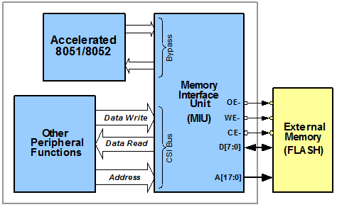
What Flash Speed Grade Do I Need to Operate the E5’s 8051 at Maximum Performance? A Triscend E5 Configurable System-on-Chip (CSoC) device has an embedded, accelerated 8051 microcontroller. The E5’s 8051 microcontroller is a superset of the original 8051 architecture. The E5 also has an improved, glueless interface to standard byte-wide Flash.
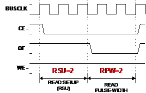
In an E5 application, the configuration data for the E5’s embedded programmable logic and the 8051application code are both stored in external Flash. The E5’s memory interface unit (MIU) provides the glueless interface to the external Flash. The MIU’s flexible timing allows you to use practically any speed Flash device. Both the read setup and read strobe timing can be programmed to be anywhere from 0.5 a bus cycle to 7.5 bus cycles. The read setup time (RSU) and the read pulse-width (RPW) are both control fields within the Memory Interface Unit control register.
However, for optimal 8051 performance, the read setup time should be set to zero (RSU = 0 = 0.5 bus clock cycles) and the read pulse-width set to two (RPW = 2 = 2.5 bus clock cycles). The result is a three bus-clock cycle read period. In order to achieve this timing, the external Flash device must have a small enough access time, as shown by the following equation.
A 20 MHz clock results in a 50 ns bus clock period. Consequently TBCYC = 50 ns. The MIU read access time, TMRAC, for an E5-25 device is 28 ns. Using the equation above …
In this example, the external Flash device must have an access time below 122 ns in order for the 8051 to operate at maximum performance.
© 2001 by Triscend Corporation. All rights reserved. |